
Quantum D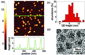 ynamics in Hybrid Materials:
There is an apparent size mismatch between modern electronic and photonic devices. While current electronic devices are routinely fabricated on the scale of tens of nanometers, photonic devices are limited to scales comparable to the wavelength of light - typically a few hundreds of nanometers - due to diffraction. We are hoping to circumvent this limitation by examining the interaction between illuminated semiconducting and metallic nanoparticles. Metallic nanoparticles (10 to 100 nm in diameter) provide the means to shaping and guiding optical fields on a smaller scale, moving beyond the diffraction limit.
In one study, we used an Atomic Force Microscope (AFM) to assemble well defined hybrid nanostructures consisting of both semiconductoring quantum dots and metallic nanoparticles. The fundamental light emitting properties of the quantum dot is drastically changed by both a modified electromagnetic environment (the “Purcell” effect) and energy transfer between the two types of nanoparticles.
Adding New Dimensions to Optical Spectroscopy:
Imagine trying to read an article with the newspaper rolled up. This is a frustrating experience as only limited information can be accessed at a glance and overlaps between the lines of the text can make it difficult to read clearly. Researchers using optical spectroscopy methods had to deal with this issue until the recent development of multi-dimensional spectroscopy. Using this new technique, we are now able to access information in two or more dimensions, unraveling previously congested one-dimensional spectra. We are one of the first groups to introduce this powerful concept to the study of semiconductors on ultrafast time scales. We hope to extend the method to the ultimate limit of studying quantum-confined structures and atomically thin layered materials.
Since the discovery of graphene, Van der Waals (vdW) materials have become one of the central schemes in materials science and condensed matter physics. These layered materials are strongly bounded within two-dimensional planes but weakly bound to adjacent layers by vdW force. Atomically thin layers can be readily exfoliated from bulk crystals, creating ultimate two-dimensional (2D) quantum materials Transition metal dichalcogenides (TMDs) which are semiconductor vdW materials that exhibit strong light-matter interaction, large excitonic oscillator strength, and binding energies, and unique spin-valley locking by optical selection rules. Using this powerful ultrafast spectroscopy technique, two- dimensional coherent spectroscopy (2DCS), we can explore the quantum coherent dynamics of the optically excited states, excitons, trions, and polarons in TMD systems. A single 2D spectrum can identify couplings between resonances, separate quantum mechanical pathways, and distinguish among many microscopic many-body interactions.
Probing Spin Dyn amics Using Light Scattering Techniques:
The spin-transfer (or spin-torque) phenomenon refers to a novel method of using an electrical current to manipulate spins in magnetic nanostructures. This effect offers unprecedented spatial and temporal control of spin distributions.
We have experimentally studied the diffraction of spin waves propagating in a Permalloy-film microwaveguide from a submicrometer-sized circular defect. For microwave excitation above the cutoff frequency of the fundamental transverse mode, the defect leads to a frequency dependent reflection of the spin wave. The efficiency of the reflection appears to be dependent on the wavelength of the incident spin wave in a nonmonotonous way. The observed two-dimensional spin wave distribution pattern after the defect can be understood based on the interference of several copropagating modes, suggesting that the defect couples the fundamental mode with higher order modes.